Turiyam AI is an India-founded semiconductor and AI infrastructure company that builds full-stack generative AI compute platforms, from silicon and systems to middleware and software. It engineers these solutions to deliver high-performance intelligence at a radically lower total cost of ownership for enterprises worldwide. At its core, the company advances an open architecture strategy: it supports open models, deploys CUDA-independent middleware, and designs RISC-V–based hardware. In doing so, it draws clear inspiration from India’s digital public infrastructure paradigm.
Turiyam AI concentrates on large-scale AI inference and positions itself to democratize access to high-performance AI for billions of users. Simultaneously, it aligns its roadmap with India’s broader ambition for technological self-reliance. Headquartered in Bengaluru and established in 2024, the company is led by a team with deep domain expertise in artificial intelligence, semiconductor design, and large-scale systems engineering.
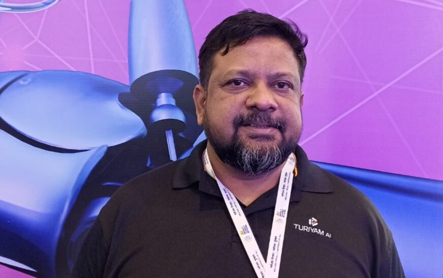
In an exclusive discussion with The Interview World at the India AI Impact Expo 2026, Sanchayan Sinha, CEO of Turiyam AI, articulates the company’s core AI inference offerings. He explains its approach to GPU design and manufacturing within next-generation AI infrastructure. Furthermore, he evaluates the trajectory of India’s AI inference market, projects AI infrastructure growth over the next five to ten years, and outlines the strategic innovations he intends to build atop the existing platform over the coming decade. What follows are the principal insights from that conversation.
Q: Could you elaborate on your AI inference offerings, and explain how does Turiyam AI contribute to the indigenization of AI infrastructure within the country?
A: We are a GPU company. We design our architecture to serve both AI training and large-scale inference. However, inference demands nearly ten times more infrastructure than training to operate at production scale. Consequently, the market requires significantly more GPUs to sustain real-world deployment.
In response, we have engineered our platform to reduce inference costs by up to 10x. As a result, enterprises can deploy AI economically across high-intensity workloads such as audio processing, video analytics, image generation, and large language models. This cost efficiency transforms previously constrained use cases into commercially viable applications.
Moreover, we control the entire technology stack. We design and build our own GPUs as an integrated part of that stack. We execute this development across our dual hubs in India and the Bay Area. Together, these teams drive our end-to-end GPU innovation strategy.
Q: Are the GPUs used in your infrastructure designed and manufactured in India, or are they sourced from international suppliers?
A: We design our GPUs in-house. However, we do not manufacture them. Instead, we rely on world-class foundry partners for fabrication. Specifically, production takes place at TSMC, the same advanced semiconductor manufacturer trusted by NVIDIA and AMD.
Accordingly, we concentrate on architecture, chip design, and system optimization, while leveraging proven global manufacturing infrastructure for fabrication at scale.
Q: How do you assess the future trajectory of the AI inference market in India amid accelerating AI adoption across industries?
A: If you examine the Indian data center market, the growth trajectory is unequivocal. At present, capacity stands at roughly 700 megawatts. However, projections indicate expansion to nearly 6 gigawatts within the next two to three years. In effect, the sector is poised for an order-of-magnitude leap.
Importantly, most of this expansion will be driven by inference workloads rather than training. India is not allocating substantial capital to large-scale AI training clusters. Only a limited number of companies are building training infrastructure domestically, and their footprint remains modest. Consequently, the bulk of new capacity will support inference at scale.
In practical terms, this implies that close to 6 gigawatts of incremental data center capacity will primarily power inference operations. Such scale translates directly into demand for inference-optimized accelerators, amounting to millions of chips across the country.
Q: Could you share the current number of active clients you are serving?
A: We currently maintain five active engagements. As a one-year-old company, we have prioritized depth over breadth. Accordingly, we have been deliberate in customer selection. We partner only with what we call “teaching customers,” organizations that provide rigorous technical feedback and help us refine product architecture, performance benchmarks, and deployment workflows.
However, this focused phase is strategic and temporary. Beginning this month, we will expand our go-to-market motion. As a result, we expect to significantly widen our customer funnel and accelerate commercial adoption.
Q: How do you envision the growth trajectory of AI infrastructure over the next five to ten years?
A: If you assess global capital allocation trends, the scale is unprecedented. The industry is currently deploying close to half a trillion dollars annually in capital expenditure, primarily toward AI training infrastructure. However, to rationalize that level of investment, the ecosystem must ultimately generate roughly five trillion dollars in downstream economic value. The capital intensity, therefore, is extraordinary, and so is the required return profile.
Moreover, infrastructure ambitions are expanding at a pace previously unseen in computing history. For example, Dario Amodei of Anthropic has articulated the need for on the order of one million TPUs to support future model development. Such figures would have been inconceivable only a few years ago. Today, they underscore the sheer magnitude and acceleration of AI infrastructure demand.
Q: What new innovations do you plan to build on top of your existing platform over the next decade?
A: We are advancing a series of architectural innovations. After all, designing and bringing a GPU to market typically requires nearly five years. Chip development moves deliberately. Consequently, the silicon shipping today reflects design decisions made half a decade ago. Meanwhile, AI research has evolved at an extraordinary pace. As a result, many recent breakthroughs in model architectures, scaling techniques, and inference optimization remain uncaptured in current-generation hardware.
We therefore see substantial headroom for improvement. Specifically, we can re-architect memory bandwidth to eliminate bottlenecks. We can expand Network-on-Chip (NoC) bandwidth to improve data movement efficiency. We can refine compute pipelines to better align with modern AI workloads. In addition, we can optimize mixed-precision execution to deliver higher performance per watt.
Collectively, these enhancements can materially reduce cost while sharpening workload specialization. In short, the next wave of GPU design must reflect today’s AI realities, not yesterday’s assumptions.