
VLSI System Design (VSD) is an open semiconductor ecosystem enabler that works to democratize chip design and accelerate semiconductor innovation. It combines industry-oriented training with open-source EDA tools, cloud-based design laboratories, FPGA and RISC-V platforms, internships, IP development, and tapeout programs. More importantly, VSD addresses the complete semiconductor design lifecycle, from RTL design, verification, synthesis, and physical design to SoC development, analog IP, static timing analysis, and silicon realization. Through this integrated approach, it enables students, professionals, academics, and startups to build practical, industry-relevant chip-design capabilities.
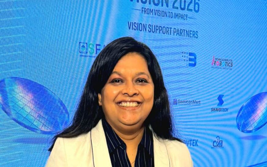
In an exclusive conversation with The Interview World, Anagha Ghosh, Co-Founder of VLSI System Design, discusses the key indicators that define the organization’s growth and impact, including learner reach, strategic partnerships, measurable outcomes, and industry adoption. She explains how VSD has opened up semiconductor education by making chip design more accessible, practical, and less intimidating for learners. She also shares the operational and commercial outcomes that marked a significant inflection point for the organization and explains why they mattered to VSD’s evolution. Looking ahead, she outlines her vision for VSD, focusing on scale, sustainable growth engines, and the capabilities required to strengthen India’s semiconductor talent and innovation ecosystem.
Here are the key takeaways from this compelling conversation.
Q: VLSI System Design (VSD) operates at the intersection of technology and education. What are the key indicators of the enterprise’s success, including learners reached, partnerships, outcomes and industry adoption?
A: VSD’s progress is best measured by the scale of our learning community and by learners moving from semiconductor fundamentals to designing working hardware and silicon. Since 2011, our mission has been to make specialised chip-design education accessible and industry relevant.
By 2021, VSD and its partners had reached approximately 56,900 unique learners across 151 countries and 53 languages through 44 online VLSI courses. Since introducing cloud-enabled design laboratories in 2017, we have delivered 14 RTL-to-GDS workshops, engaging more than 35,000 participants. Since 2020, our 17 open-source hackathon series have attracted more than 24,800 participants.
We also measure success through technical outcomes. Community designers submitted 62 projects for manufacturing through Google-sponsored SKY130 shuttle programmes. Our mentorship has supported more than 50 analog and digital semiconductor intellectual-property blocks, with more than 20 progressing to silicon.
We launched VSDOpen, our online semiconductor conference, in 2018 and introduced the VSDSquadron hardware platform in 2023. Today, institutions approach us for laboratories, curricula and tapeout programmes that help learners take completed chip designs towards manufacturing. This demand shows that VSD has evolved into a platform spanning education, design, hardware and silicon.
Q: Semiconductors can appear highly specialised and inaccessible. How did you make the subject more open, practical and less intimidating for learners? How has that approach translated into tangible enterprise advantage?
A: We made semiconductor learning accessible by combining open-source tools, cloud-based laboratories and structured, project-driven learning. We move learners from fundamentals into design, simulation, verification, hardware implementation and chip manufacturing.
We designed the underlying platform to serve multiple audiences. A school student can start with digital logic. An engineering student can progress through a complete chip-design flow. A university can integrate the same infrastructure into its curriculum. The depth changes, but the platform remains reusable.
That model creates a path from an initial workshop to a laboratory deployment, hardware programme or broader institutional engagement. It also allows us to serve additional customers without rebuilding the delivery infrastructure for every engagement. This lets us expand while maintaining consistency and quality.
Learner projects and community feedback continuously inform our programmes. Practical outcomes strengthen customer value, while reusable infrastructure supports scale.
Q: What did you have to learn about finance and business growth that technical expertise alone could not teach you? Could you share the commercial or operational result and why it became an inflection point?
A: The most important lesson was that revenue growth alone does not create a scalable enterprise. In our early years, every new batch demanded additional teaching, mentoring, support and operational effort from a small team. Technical expertise could create demand, but our ability to fulfil it remained tied to the founders’ time.
The inflection point came when we recognised that we had to convert expertise into assets that could create value repeatedly. We invested in structured learning modules, cloud laboratories, standardised curricula, open-source design flows and, eventually, the VSDSquadron hardware platform.
This changed how I evaluated the business. A programme could generate immediate revenue, but the infrastructure behind it could support multiple audiences and create future opportunities. I learned to measure not only current income, but also the long-term value and scalability of what we were building.
Operationally, this shift allowed us to expand delivery without either co-founder participating in every engagement. Commercially, a workshop could become the entry point for a broader institutional relationship. Building repeatable capabilities proved more transformative than simply increasing the number of classes we delivered.
Q: Looking ahead three to five years, what is your vision for VLSI System Design (VSD), reflecting about scale, growth engines and the capabilities or capital required?
A: Our vision is to build VSD into an integrated semiconductor ecosystem connecting early learning, advanced design skills, hardware development and indigenous silicon. We want learners to progress from their first chip-design lesson to contributing to products conceived in India for global markets.
Our next growth engines are semiconductor laboratories, cloud-based learning, the VSDSquadron hardware platform, industry programmes, and indigenous IP and chip development. These initiatives build on infrastructure already developed. Our objective is to increase adoption while enabling more community projects to progress from design to tapeout and working silicon.
Institutional programmes and hardware platforms will be central to this expansion. We want universities to provide practical semiconductor design experience, so learners develop capabilities they can apply directly in industry. We also intend to widen participation, particularly among women and learners outside established technology centres.
Ultimately, I measure success by more than revenue or enrolment. I want to build an enterprise that combines sustainable growth with a measurable contribution to India’s semiconductor talent, design capability and indigenous silicon for global markets and the country.