
Tokyo Electron Limited (TEL), founded in 1963 and headquartered in Tokyo, Japan, is a global leader in semiconductor production equipment. The company develops, manufactures, and sells advanced systems that support critical stages of semiconductor manufacturing, including deposition, coating and development, etching, cleaning, and wafer testing. These technologies help chipmakers produce increasingly advanced, high-performance, and energy-efficient semiconductors that power today’s electronics and digital infrastructure. The company continues to advance semiconductor manufacturing through artificial intelligence, robotics, advanced packaging, automation, and sustainable technologies. At the same time, TEL remains focused on strengthening innovation across the semiconductor value chain.
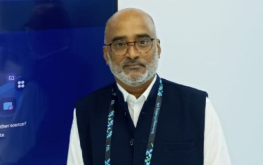
In an exclusive conversation with The Interview World at SEMICON India 2026, Vaidya Bharadwaj, Project Leader, TEL India Project, Tokyo Electron Limited, discusses TEL’s key product lines and evaluates India’s growing semiconductor market potential. He explains how TEL supports leading companies developing and manufacturing advanced AI chipsets at scale. He also outlines his vision for innovation over the next three to five years, highlights measurable performance benefits from TEL’s automation solutions, and examines the Government of India’s role in accelerating semiconductor manufacturing. Here are the key takeaways from the conversation.
Q: What are Tokyo Electron’s key product lines, and how do you assess India’s market potential, opportunities, and growth prospects for TEL?
A: India represents a potentially significant market for us in the future, and we have been looking forward to establishing a stronger presence here for a long time. We see substantial opportunities, supported by the market’s scale and, importantly, the stability and consistency of government policies. Over the years, we have also witnessed considerable progress in India’s semiconductor ecosystem.
Tata Electronics will be a key customer for us in India. We are proud to be its first MOU partner, and we will supply and deploy multiple product lines at its upcoming fab in Dholera.
Our portfolio will cover several critical semiconductor manufacturing processes. For lithography, we will provide our track and coater/developer systems. For deposition, we will supply ALD and furnace equipment. We will also provide etch solutions for back-end and interconnect applications, along with wet-clean and wet-etch systems.
In addition, we will supply probers for final product testing and yield verification. Through this broad portfolio, we look forward to working closely with Tata Electronics and supporting the development of India’s semiconductor manufacturing capabilities.
Q: What semiconductor manufacturing solutions do you offer to support leading companies developing and producing advanced AI chipsets at scale?
A: AI is still at the beginning of its evolution, and its impact on semiconductor technology is already reshaping the industry. Traditionally, chip innovation has focused largely on process-node scaling and transistor-level shrinkage. AI, however, is driving a broader shift toward system-level optimization and co-optimization.
As a result, we are seeing tighter integration between logic and memory, while memory architectures themselves are advancing rapidly through technologies such as high-bandwidth memory (HBM) stacking. We provide tools across this evolving landscape, supporting both logic and memory processing at the chip level.
Our capabilities also extend to advanced packaging, where we offer bonding and debonding systems, polishing and trimming tools, and advanced probing solutions. This gives us a comprehensive technology portfolio spanning the semiconductor value chain, from chip fabrication to advanced packaging. As India strengthens its semiconductor ecosystem, we are keen to see how its advanced-packaging capabilities evolve and where new opportunities emerge.
Q: What is your vision for innovation over the next three to five years, and which breakthrough products or technologies will define it?
A: We will continue investing in technology, particularly chamber-level technologies that enable us to advance toward leading-edge nodes. This includes both advanced logic and memory nodes, where we will sustain our focus on innovation and process advancement.
At the same time, we will expand our focus on advanced packaging and develop new products as semiconductor architectures evolve rapidly. Beyond technology development, we will accelerate automation and digital transformation across our operations.
Our objective is to minimize or eliminate manual errors and ease workload associated with tool maintenance, including preventive maintenance and routine parts replacement. We will increasingly deploy automation and robotics to perform these activities.
In parallel, we will introduce digital solutions that extract actionable data from customer tools and apply agentic AI to predict tool performance and health. These systems will also generate recommendations to improve performance, increase uptime, and strengthen operational efficiency. Together, these investments will deliver measurable value to customers, particularly large, technology-intensive clients.
Q: What measurable benefits and performance metrics can Indian enterprise clients expect from your automation solutions in terms of efficiency, cost savings, and growth?
A: We have been steadily advancing automation, while increasing the software intelligence embedded in our equipment. However, semiconductor manufacturing is now expanding at unprecedented speed, and the industry faces a growing shortage of skilled resources. We therefore need to do more to reduce the burden on our customers and make manufacturing less labour-intensive.
Automation is a critical part of that solution. It can simplify complex maintenance procedures and improve consistency across critical processes. When engineers open a chamber and service these highly sophisticated systems, outcomes can vary. Our objective is to increase the success rate and make maintenance more predictable by using automation to assist human operators, reduce complexity, and improve execution.
At the same time, automation can help customers reduce labour-intensive workloads, improve operational efficiency, and accelerate fab ramps. Ultimately, faster and more reliable operations will enable faster chip ramps, allowing customers to bring products to market significantly sooner.
Q: How do you assess the Government of India’s role in accelerating semiconductor manufacturing, particularly chip production, and strengthening India’s position in the global semiconductor ecosystem?
A: At the opening ceremony of SEMICON India 2026, our CEO highlighted the transformative potential of semiconductors and the critical role of the Government of India in realizing this opportunity. As Prime Minister Modi has emphasized, semiconductors are the “digital diamonds” and the “new oil” of the modern economy. More importantly, they are a pervasive technology that will underpin virtually every sector.
India has the talent, capabilities, and potential to become a significant semiconductor hub. Over the past four years, the Government of India has pursued a consistent policy approach to develop the industry, strengthen the ecosystem, and establish a durable foundation for growth. Its contribution extends well beyond financial support. It includes policy direction, regulatory facilitation, infrastructure development, and institutional coordination.
Building a fab is only the beginning. A globally competitive semiconductor ecosystem requires an entire industrial city around it. Prime Minister Modi’s vision of creating a city comparable to Hsinchu is already taking shape. Airports and highways are ready, while rail connectivity, hotels, housing, schools, and hospitals are being developed alongside the semiconductor infrastructure.
In most established semiconductor hubs, this surrounding infrastructure already exists. India, however, is building the ecosystem almost from the ground up. Therefore, sustained government support is not merely valuable, it is fundamental to making this vision feasible.